


Backside Power Delivery and Bold Bets at Intel
Architecture bets that Intel and TSMC are making
Backside Power Delivery
I listened to the “New Ways to Wire and Integrate Chips” master class by Applied, and it was a eureka moment for me. If you have time, I would watch the event yourself. Applied Materials talked about wiring in chips and the industry's problems with scaling to smaller transistors. The conclusion is that the backside power delivery trend is the next leg of how logic chips shrink.
EUV was a big technology change in the 7nm era, but the continued size shrink afforded by EUV is helpful but not the only solution to the challenges of scaling. The big opportunity that Applied talked about extensively is backside power delivery network (BS-PDN). BS-PDN is such a big deal you might as well call this the extension beyond Gate All Around (GAA) to 1/2nm nodes. The roadmaps of both Intel and TSMC’s competitiveness hinge heavily on BS-PDN implementations. It’s not hyperbole to say the entire Intel turnaround hinges on this technology. So let's learn exactly what it is.
Backside Power Delivery Network is attempting to fix one of the big problems in transistor scaling; energy. There is a resistance problem which is a fundamental problem in electrical engineering. A friendly reminder for readers that resistance is a property of how strongly the material resists electrical current. Resistance for materials like Copper has never been a limiter, but as we scale copper wires smaller, the resistance is starting to rise exponentially.

The intermediate solution was new metal layers such as Cobalt. Cobalt helped these wires maintain enough charge to carry signals and power to the transistors to work, however this relationship is reaching a fundamental limit. And it’s kind of hampering the ability to make smaller transistors all together.

Moving electricity throughout the package is one of the most important from an energy perspective, as this impacts the total performance and power of the semiconductor. Beyond the resistance challenges of semiconductors at the microlevel, we are likely hitting the limit of complexity at the power distribution layers in a typical semiconductor. A standard semiconductor is built up layer on layer on the front side of the wafer, which is how we’ve been scaling for a long time. There are many layers of metal distribution networks, and now the IR (resistance) drop is starting to become cumulative and too much to handle.

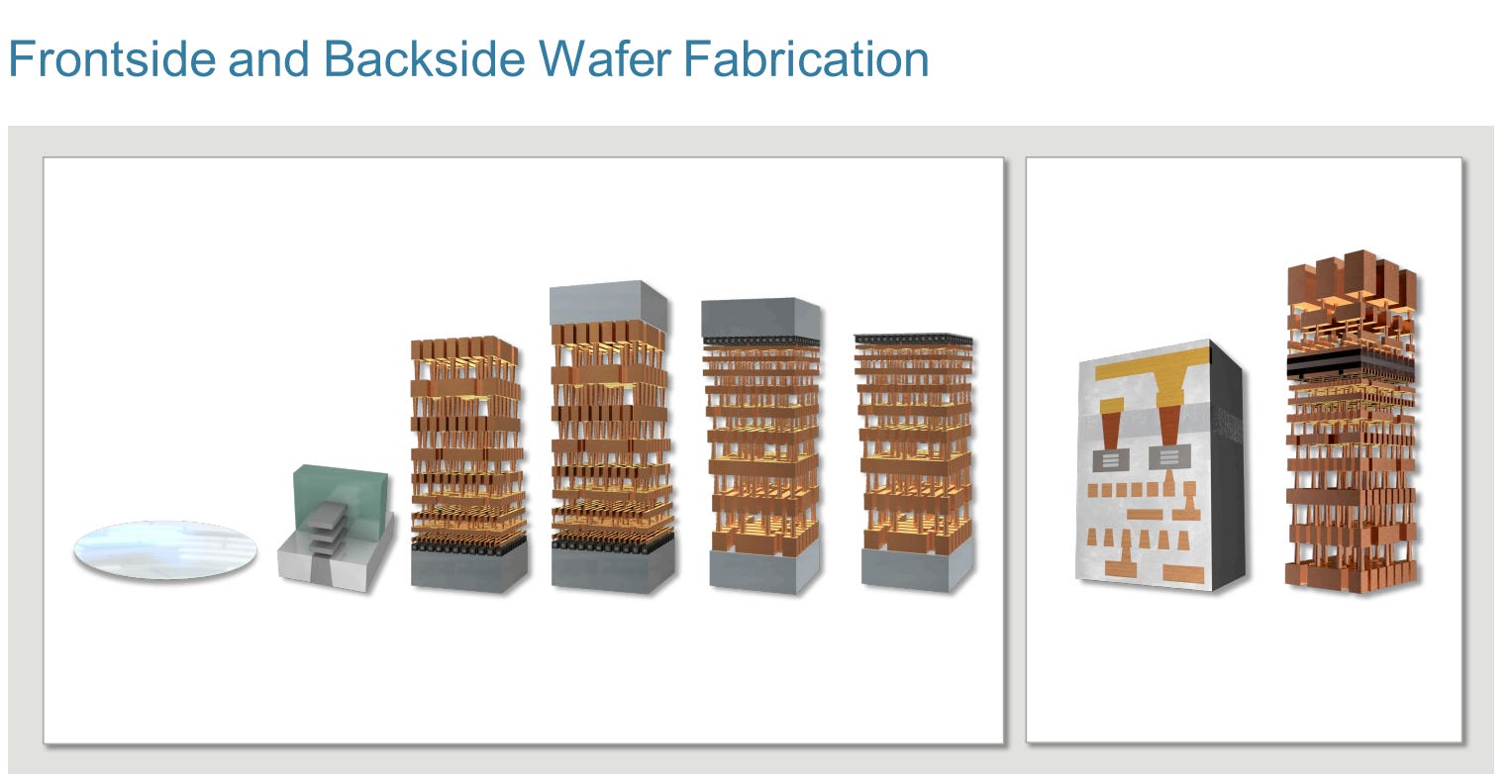
The successive layers cause a voltage drop, and the higher resistance compounds this with smaller layers. These background layers in a semiconductor are essential for the total design of the most critical layer - the actual transistor itself. SO we can’t make these massive stacks on the front side anymore, so what are we to do? Well, this is where a Backside Power Delivery Network comes into play. It’s a clever trick to split the signal and power layers that should scale transistor size more than the physical shrinking of the geometric features. So we are reorganizing the inside of the semiconductor structure. Below is an example of how the BS-PDN would shrink the structure size.

Removing the power signal and signal line to just a signal line would free up space for more transistors. This is an effective shrink using creativity instead of fundamental physics. BS-PDN would achieve this by putting the signal layers on the top side of the chip and the power layers on the bottom side of the chip.
This new technique has never been before but is a continued extension of the advanced packaging trend. Traditionally we have been building semiconductors only on one side, but now we have begun to bond chips together using Hybrid Bonding. Engineers realized that we could bond the power layers to the underside of the chip and save space and solve the resistance problem.
The net effect is a way to scale transistor size that doesn’t rely on EUV, and what’s more, this shrink will be the equivalent of 2 generations of EUV shrinkage.. That’s huge and now it’s pretty much the roadmap for future semiconductor scaling.

Notice the shift from planar to FinFET, to GAA (to come), and eventually GAA with BS-PDN. Again, lower area and better efficiency are scaling a chip, and this time the shrink is not coming from lithography but an advanced packaging technique! How far the advanced packaging trend has come.
But if you’re paying a bit closer attention to the Applied Materials presentation, they talk about how there are different ways to implement BS-PDN layers. They put a good, better, best of Buried Side Rails, Power Via, and Backside Contact to Source/Drain. The difference between techniques is orders of magnitude different, with backside buried rails offering a 7X better power performance than front-side delivery. So how aggressive you are on this path will reap enormous rewards for your potential chip.

If you’ve heard Power Via before, that’s because Intel plans to all in on it. In 2024 when they ship the 20A node, they will insert Power Via BS-PDN alongside RibbonFET, and the net effect is that they should take process leadership. I don’t think RibbonFET alone would be enough, but TSMC’s chosen implementation of BS-PDN is the low-complexity Buried Power Rail. This is the real bet that Pat Gelsinger and Intel make on their architecture. Putting aside recent Sapphire Rapids execution issues (sigh), I can finally see the “how” Intel turns it around. It’s about a more aggressive BS-PDN choice than TSMC while offering GAA.
TSMC likely will not fail, given that Buried Power Rail can be done on today’s tools, while PowerVia is a technology that hasn’t been implemented yet. So TSMC in typical fashion will execute on conservative but achievable architecture choices, while Intel is betting the farm on BS-PDN.
BS-PDN is a huge inflection point. If Intel lost its lead to TSMC when they failed to insert EUV early enough, this is where TSMC could lose its lead in transistor density by not taking aggressive design moves to improve performance. I cannot overstate this specific decision's importance (along with RibbonFET, but both companies will have GAA at that point). But I’m not going to leave it off just there yet.
These changes are small between the two companies, but these are in effect billion-dollar bets on who's going to make the best technology. This is unlike traditional scaling and previews what’s to come. EUV came and helped shrink, but now it’s going to not just EUV but also design choices like BS-PDN. This entire methodology even has a new name, Design Technology Co-Optimization or DTCO.
As I wrote in “The Rising Tide of Semiconductor Cost”, it isn’t just about scaling size anymore. DTCO is a perfect example of why fabrication is getting more expensive, and these technical challenges are going to be how we scale going forward. This handy graph shows the percentage DTCO leads to density scaling.

DTCO will go from clever changes to the de-facto way to scale semis. This will add incremental costs and design that will make the chip more expensive and complex to design but significantly add more steps and processes to making a semiconductor. The complexity, of course, is suitable for semicap.
Additionally, the specific mechanism of how we improve scaling is a form of advanced packaging on the micro-level - and that’s by wafer to wafer bonding through hybrid bonding to flip two chips into a single die. BS-PDN is just the first example we’ve seen in the scaling process. The big winner and new technology here is hybrid bonding. Below is the old interconnect method on the left and the new one on the right.
If you look at the right-hand graphic, you can see that black and grey metal layer, the hybrid bonding layer that will merge two die together to create the backside network and separate the signal and transistor level. In addition to solving the resistance problem, the other benefit here is the cell size will be smaller. Look at the before and after if you remove the power rail. It’s a 20-30% cell area reduction!

What’s amazing is there is a roadmap as well, as BPR scales to PowerVia, which then scales to Backside Contact Source/Drain. The other huge takeaway here is hybrid bonding will be a big deal, and this effect will add more silicon, more steps, and a whole new and highly critical tool that will matter. Wafer-to-wafer and Die to wafer tools will matter immensely.

Many companies are pursuing this - including Applied Materials with a Die-to-Wafer tool in conjunction with BESI. But let’s not forget about Wafer to Wafer, a new tool offered by Tokyo Electron. These markets are substantial incremental growth drivers, and the wiring opportunity is expected to grow at 3x the rate of WFE! Finding the semicap companies most levered to this trend will be a considerable advantage for relative fundamental outperformance in semicap.

These design choices are the next big leg that will propel us forward. EUV is here, and High-NA will help with resolution errors, but it’s not as simple as thinking about things in a EUV-only context. The next leg will be more advanced packaging-type innovations in the fabrication process. This is yet another secular insertion into the semiconductor process. The fate of the two largest fabs is hinging on an advanced packaging decision, not a lithography decision, and likely separate advanced packaging decisions will be the driver beyond just BS-PDN type decisions.
The ability to make the best multi-chip package is the next frontier of competition. It solves the reticle problem and will likely solve multiple issues for technology scaling as the world becomes more specialized. Hybrid bonding is the tool that makes it all possible. BS-PDN, hybrid bonding, and DTCO are just signs of what’s to come.

Hey guys! It’s been a bit of a week, but I have a few posts coming up. I hope to write something akin to a CXL primer and an overview of AMD IR day next week. Maybe BESI and KLAC if I have time as well. It’s been a bit, but I’m brimming with ideas. Talk to you soon.
Wow - best article on BS-PDN & Hybrid Bonding I have read thus far. Truly a f(x) change in the future of semi design - incredibly impt for both investors & engineers(although I think the engineers have known about this for a while, investors maybe not so much hah). Thanks for researching and writing.
Would love to hear your thoughts on the KLA investor day - some interesting things said. Particularly around cost per transistor declining from 10 nm to 2nm & number of wafer starts per month on 7nm is 2.2x vs 10nm (I wonder what wafer starts per month on 3nm is relative to 5nm and how trend continues). Interesting implications for the materials ecosystem && the longer shelf life of nodes resultant from EVs & hyperscalers is interesting in context of the tool makers.