Metrology Primer
The next of a series of primers in semicap manufacturing.
I finally continue the Semicap Primer Series! If you’ve been reading the newsletter at all as of late all I have been talking about is Metrology and Inspection. So, without further ado – let’s dive a bit deeper into what metrology and inspection mean.
As a quick reminder, Metrology and inspection are a meta-step in the fabrication process. Outside of patterning, deposition, etch, cleaning, metrology and inspection are the act of measuring the effectiveness of these previous steps. Inspection and Metrology are often called “process control”, and are a meta-process of quality control that is interwoven between all the process steps.
First by answering one of the hardest distinctions that I still get confused about and that is what exactly is the difference between the two?
Metrology vs Inspection
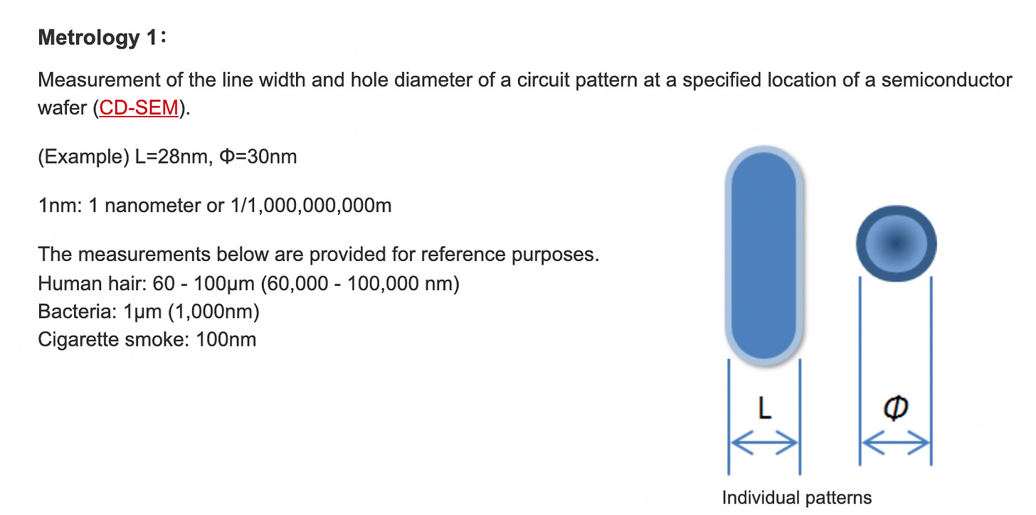
Metrology in its broadest sense of the word is the science of measurement and its application. In the case of semiconductors, it’s the science of measuring the wafer and critical dimensions of the chip to make sure it’s correct. It is a form of Process Control – a phrase used to talk about all kinds of measures taken by fabs to ensure uniformity, fewer mistakes, and the correct processes. Metrology is often a series of samples on the wafer to ensure that the manufacturing process is correct. This graphic by Hitachi Hi-Tech nails it.
Most of these are measurements to check to see this semiconductor is working as it should be. Now let’s move on to the very similar but slightly different category of inspection.
Inspection is using devices to inspect wafers and masks for defects. The two are so confusing because well Inspection is another form of process control and similar to metrology. However, in this case, it is in the form of looking actively over the wafer and finding results. Metrology is a passive result quality control method, akin to measuring a dimension for variance. Inspection is actively looking for things with a fine-tooth comb – trying to find exactly where the defect lies and why.
When comparing the two I really think my favorite analogy is calling metrology a routine police patrol while an inspection is more akin to investigating the scene of a crime and looking for the murder weapon.
So in this analogy metrology is trying to stop routine but common mistakes from happening. This is mostly done by comparing the expected result of a peaceful neighborhood to the actual neighborhood. These kinds of routine patrols prevent persistent crime (or defects) to creep into day-to-day life. Inspection is a much finer process of looking at what exactly caused what. Both are obviously important in the process of day-to-day defect management.
Why Metrology and Inspection Should Do Well
I wrote a lot more about this in “Rising Cost of a Semiconductor” – in particular, that the yield math is one of the most compelling arguments for the need for more metrology. The cost of defect failures is starting to spiral out of control, and the cheapest insurance against this is more Metrology and Inspection. One of the changes the industry is adopting is advanced packaging as the primary driver to increasing semiconductor performance. The push to advanced packaging has an entire set of consequences, namely newer packaging technology and a new vector of failure.
Additionally, Metrology and Inspection spending tends to ramp before the rest of the tools, and that is why they should continue to grow so robustly in 2022 given that large fabs are just starting to come online. Metrology and inspection ramps are likely happening currently for the N3 and N5 nodes at TSMC and Intel.
In my view, there are two drivers of metrology and inspection intensity increasing. The first is that leading-edge processes continue to be demanding and the cost of failure is very high. This should at least grow with WFE. The second is the rise of increasing complexity in the backend driven by advanced packaging, and this should grow faster than WFE.
Front End Metrology
Metrology intensity rises for the most part in-line with the number of steps of a semiconductor. That is to say that metrology intensity is likely going to rise in line with semicap intensity. Metrology and process control is, unfortunately, an insurance product, and is only bought when yields become increasingly hard. Given the increasing complexity of semiconductor manufacturing, it makes sense that metrology and inspection should rise at least as much as the other areas of semicap.
I love this slide from KLAC. The margin of error is very low. This slide from KLA points out that a 99.5% rate of success would be a complete failure after the ~1000 non-metrology steps needed to make a modern semiconductor. Essentially the manufacturing process requires perfection.
Given that the increasing number of steps and complexity is a trend that will not be stopping, metrology should increase in-line or possibly a bit more as yield challenges make ramping more complex nodes harder. The real kicker for increasing complexity in my opinion is more on the backend, where the density of pitches and cost of failure is spiraling out of control. The risk of a large and expensive finished good failing because of relatively cheap packaging technology is making the cost of insurance rise steeply.
Back End Metrology
Advanced packaging is of course the big focus area for semiconductors. Each of the new techniques such as fine pitch flip-chip, fan-out wafer-level packaging, and hybrid bonding are additive to the manufacturing process. (For a very good and recent primer written about the types of Advanced Packaging refer to Dylan’s latest series).
These costs are additive to making a semiconductor and extend beyond just the traditional front-end processes. This is additive to the total cost of making a semiconductor package. The problem lies when you have an expensive piece of semi-finished goods being bonded together in increasingly expensive processes that require precision. The precision for metrology and inspection is increasing and that demand is moving metrology demand higher.
The cost of 1 expensive die in a multi-chip module failing because of a relatively cheap misplaced micro-bump could ruin the entire package, and this is why the cost of failure is increasing and thus “insurance” of metrology and inspection is rising in the BOEL (Back end of line). In addition to the logic of “insurance” being important, the entire category is one of the largest incremental growth categories within the entire semiconductor fabrication process.
Advanced Packaging is a huge catalyst for more Process Control, and for once I believe that Metrology is going from a “nice to have” and cost center to a strategic focus in the front end. A pretty simple illustration of the impact of effective yield per chiplet shows a pretty startling impact of the yield – it’s going to have to be higher for an effective yield to be acceptable. Note the similarity to the previous slide from KLA.
Technical Dive
Okay after explaining to you at a high level about metrology – I want to take a bit of a deeper dive. If you want to skip this and go to the company overviews I fully understand – this is primarily if you want to learn a bit more about how and why metrology and inspection work.
I want to preface that most of this is a lagging edge from a 2000 era textbook. In interviews and conversations with experts, I’ve gotten that most of these core assumptions have stayed the same but are just operating on a smaller scale – so let’s explain some of the major steps in the metrology and inspection process.
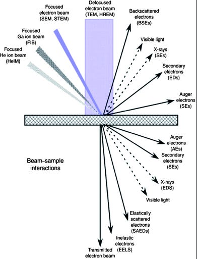
At a high level, all of inspection and metrology can be simplified as a source of electrons, X-rays, or light hitting a sample and then collecting either secondary electrons, x-rays, or other data from that interaction. That is the core technique of metrology and inspection. Some of the light or electrons pass through, some are bounced off the surface. The information collected from these secondary results can tell a meaningful amount of the sample. This is the core mechanic of both inspection and metrology processes.
This is a core graphic. First notice the beam sources (TEM, HREM, SEM, STEM, FIB, HeIM) creating secondary electrons, x-rays, or other secondary particles that can be measured. The interaction effects of these particles with the sample create a large amount of information that can be used to then create inferences about the dimension, material, and other properties of the sample.
The raw data from this process however is not enough to understand what an engineer is looking at, it actually takes a large amount of model-based simulation and experimentation to create a model that then better reflects reality. In my estimation, there is a meaningful cumulative advantage from creating solutions in metrology because it isn’t just the physical tools but the models of reality itself in conjunction that creates the solution. Creating the model from scratch takes a lot of effort, data, time series, and other factors for various methods of metrology and inspection.
Now next there are different times metrology and inspection are used. In-situ versus standalone. Both have their places, but I would say the difference is that in-situ is within a series of chambers or part of the chamber process, while standalone is a separate machine that is larger and more accurate. In a perfect world, everything would be in-situ, but the reality is that standalone machines are needed.
In-situ - “In process”, and often used to improve the performance of a chamber or step. Think of this as double-checking your work on the fly.
Standalone Metrology/Inspection - This is a standalone machine. The reason for standalone machines is that the stage, angle, precision, and throughput are much better in a standalone process. It makes sense to separate the processes as some of the processes can be messy or even destructive.
Ebeam or Not to Ebeam
Another area I want to talk about is Ebeam versus optical. Ebeam is a process of pushing primary electrons towards a wafer in a tight beam, hence an electron beam. This ebeam process creates secondary electrons and backscattered electrons. Secondary electrons are measured from the same side as the beam and are sensitive to the surface, while backscattered electrons are measured on the backside. Secondary electrons are better at surface information, while back scattered electrons tell more information about the composition of the sample.
The net effect is a high-resolution image-based inspection method. This works to resolution levels lower than optical methods and importantly has a roadmap to scale. The only real problem is throughput, as ebeam is a focused beam with lower throughput and higher resolution.
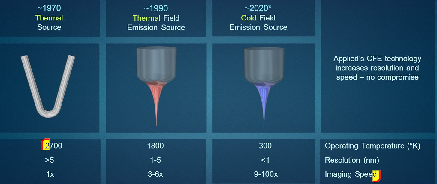
The part that would make Ebeam more competitive is throughput increases. This is currently being worked on by Applied, KLAC, and ASML. However ebeam is still orders of magnitude behind.
Recent throughput increases by the likes of Applied Materials have managed to increase throughput, but Ebeam still is orders of magnitude behind Optical inspection. Ebeam adoption will increase regardless, as the resolution offered will matter for 3nm and below.
However, the reality I’ve come to realize is that Ebeam and Optical are both going to exist for a long time. There is a direct complementary aspect of optical. Optical in particular is well suited for wafer to wafer variation and systematic defects, aka Metrology. While Ebeam is going to be a larger portion of inspection for leading-edge sub 7nm logic.
One of the big takeaways is that while Ebeam is clearly a runaway growth category in the short term as it creates a larger addressable market, however, it doesn’t come at the expense of optical strictly. Optical inspection is likely going to be used less, but Optical itself is not going away. Both are just different tools, and both are in high demand as scaling becomes harder.
Optical is Not Constrained in Metrology
The last thing I want to talk about is the misnomer of the limitations of optical technology. When I started this dive I was under the assumption due to the size of the pitches optical technology was going to start hitting the wall of the light being larger than the feature the machine was inspecting.
This is not a limitation as I first thought. The primary reason for this is scatterometry, which is measuring the trajectory and polarization of light after it hits a surface. Think of modern optical techniques as bouncing light off a surface and measuring the angle of light scattering to create inferences about the sample.
By systematically bombarding a surface with optical light you can find a lot of information about the underlying, even if the sample is larger than the light source you’re bombarding the sample with. That is the modern state of optical, and it seems like this can scale for a meaningful while yet at an extremely cost-effective rate with higher throughput. Importantly this method is model-based, meaning that the bouncing of the lights has to be interpolated with a meaningful amount of data and modeling experience. There is a cumulative advantage here, as entrants in optical model-based inspection seem unlikely.
In particular when a large percentage of the sample has to be measured optical really shines. In this case, Metrology will likely be optical-based for a long time yet, while inspection will continue to pursue ebeam and other non-optical-based methods.
Overview of Types of Metrology and Inspection
Now I want to start to move onto the common “types” of metrology and inspection. The thing I want to focus on is that while each has specific applications they are often used for, the reality is multiple methods can achieve the same results. Oftentimes choosing between a CD-SEM and OCD film techniques doesn’t really matter, because both are good enough for the job. The choice and trade off for why each technique gets selected is something process engineers decide, based on the risks and benefits of each type process.
First let’s start with the original inspection and metrology method, CD-SEM.
CD-SEM - Critical Dimension Scanning Electron Microscope
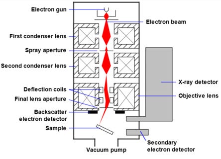
CD-SEM is an electron beam that is scanned onto the surface of a wafer and the interaction of the measurement of the surface topology generates data that gives information about the materials.
It’s important to note that SEM is not a camera but a beam that creates information about a surface and then is collected. When these electrons interact with a sample it creates multiple electrons as a result which can then be measured and create an image. CD-SEM is one of the most common forms of inspection and metrology.
TEM - Transmission electron microscope
A transmission electron microscope is similar to CD-SEM, but is more focused on transmitted electrons that pass through a sample to create an image. This obviously is useful to create multi-layer deep images for semiconductor manufacturing. TEM and SEM can be used in conjunction to become STEM. One of the bigger problems with TEM is the field of view can be limited, as well as the interaction between SEM and TEM can create noise.
This is a method of directing light on a sample and measuring photo-excitation. By adding light to the sample, the material can jump to higher electronic states and release photons. This can give insight into the optoelectronic properties of semiconductors and is a measure of the outer orbitals of a material’s electrons.
X-RAY Diffraction (XRD)
This is a method to measure the three-dimensional structure of a semiconductor. It’s used to measure the atomic structures of crystal structure and is thus helpful for semiconductor manufacturing metrology. It’s primarily used for materials metrology.
X-RAY Fluorescence (XRF)
This is another material and chemical metrology process. After the bombardment of high-energy x-ray, the secondary x-ray expels electrons that can be used to create information about their underlying composition. Again for materials metrology.
XRR focuses on the amount of reflection of X-ray beams from a high-energy source. Reflectometry can be used to characterize structures in the semiconductor manufacturing process. Hint once again another materials metrology product.
XPS spectra are obtained by exposing the film of interest to a primary x-ray which can either be absorbed by the material or scattered through the material. If the x-ray is energetic enough, it is absorbed and transfers energy to an inner shell electron. The electrons emitted because of this incident x-ray will have kinetic energy that is representative of the chemical signature of the element. Analysis of this photoelectric effect is known as XPS. (This is straight from the Nova Instruments website)
This is primarily a process of light scattering. By measuring the scattering of light you can find a fingerprint of the underlying materials and chemical composition. Raman measures the change of polarization of light to find characteristics such as strain, crystallinity, phases, grain size, and composition. This is a non-destructive and optical process.
FTIR or Fourier transform infrared spectroscopy relies on Infrared light instead. By measuring the reflection and absorption of light you can find the frequency that is associated with each chemical bond. This is a complementary process to Raman Spectroscopy.
An optical method for thin-film measurements. MBIR is importantly model-based and uses infrared light instead of other visible spectrum light to create measurements.
Not a specific method, but rather an optical tool that is used to find the dielectric properties of a film. An ellipsometer emits light, polarizes it, and after the beam is reflected from the surface it measures the polarization of light. This is an indirect method.
Focused Ion Beams is similar to a scanning electron beam but rather than a large light source it uses an extremely focused beam of ions. Since the beam of ions are focused, it hits the surface and sputters a
Optical CD is based on scatterometry-based OCD to provide 3-D information to characterize structures. By shining a light on a film and measuring the scattered light and polarization, OCD can characterize the structure on a very cost-efficient basis.
Important to note that Atomic Force Microscope is a destructive process. AFM drags a probe across the surface of a sample and then measures the debris and other products that sputter off the face of the product. This is a destructive practice so it’s mostly used in scaling process but not for high volume manufacturing.
Laser Acoustic
This is an interesting and niche metrology tool. Primarily through the Metapulse tool (Onto), you ping a sample with a laser and then measure the acoustic vibration of the material using sensors. This is used for metal composition metrology.
This is how an inspection can “see-through” a sample. When a surface is bombarded with electrons, some electrons slip through orbitals and inevitably penetrate a sample and come out the backside of the sample. This is backscatter diffraction, and by collecting this information you can create information about the sample’s crystalline structure.
Conclusions
Sadly this is not an exhaustive list of the entire processes used for metrology and inspection. I wanted to introduce you to some of the most basic forms of inspection and metrology and open your eyes to the variety and types of meta-information created from each source of light, x-ray, infrared light, or electron beam.
The primary problem is that many tools actually use multiple techniques in conjunction to create solutions that fit the exact use case of the semiconductor production step. For example for measuring a thin film, both CD-SEM and OCD work, but one or another gets chosen depending on the process and tool qualities. Put differently there are many different sets of tools that can do the same job, and it’s the job of the companies themselves to bring the best solution to solve the problem at hand.
Even Ebeam, the notorious disruptor technology will not “kill” optical, just widen the breadth of tools that a process engineer has at their disposal.
For more analysis on specific company product portfolios and what each public company is levered to, as well as an almost exhaustive list of metrology tools, refer to the rest of the section behind the paywall.


