
Semicon West: Big Shifts in the NAND Market
Tokyo Electron's New Etch Tool: Cryogenic Etch
Semicon West is “back”! Participation this year was up 65% compared to 2022, and I believe it’s an all-time high for visitors! Over 25,000 attendees came to Semicon this year, and that’s the best sign that semiconductor manufacturing in the US is back! Amid Applied Material’s new tool Vistara, Lam Research talking about their simulation platform, and Tokyo Electron talking about a new etch tool, there was a flurry of news and product announcements.
The most exciting piece of news is Tokyo Electron’s cryogenic etch product. Their new product is a big deal. Their third generation of cryogenic etch is making big waves in the market. Let’s first briefly discuss etch, and then I’ll talk about what’s the big deal with Tokyo Electron’s new tool.
What is Etch?
Etch is a process of removing material in a semiconductor structure. It’s intertwined deeply with lithography and is the follow-through of the lithography process for making a chip. After the lithographic process, the pattern is washed away, and further material is removed in the etch process. Below is a great summary of the process.

Etch comes in two types, dry and wet etching. The type is dependent on the materials in use. Wet Etch uses liquid chemicals to remove materials. In contrast, dry etch uses gases or plasma to remove material. Wet etch is isotropic, meaning it goes in all directions equally. A dry etch can etch into a single direction because the gas can be forced in a direction.
The tool in question is a dry etch tool and uses a hydro fluoride (HF) gas to etch a long deep trench into a semiconductor material. So what’s the exact big deal with the new tool?
What’s the Deal with Tokyo Electron’s New Tool?
This tool has been coming long and differs from the conventional etch process. First, the process is cryogenic, which means it’s being done with an integrated cooler, and the process is at -70 Celsius, compared to the normal process being conducted at 0-20 Celsius. Cryogenic etch is not new and has been around in research papers since the 1980s.
However, there wasn’t a need until very recently, and Tokyo Electron has been focused on bringing this technology to production. This is the third generation of cryogenic etch, and it seems like it’s finally time for the big time.

The key enabler here is that by lowering the chamber's temperature and process, they can have more etchant gas in the process, improving critical dimensions, depth, selectivity, and time. These are all huge improvements over the conventional process.
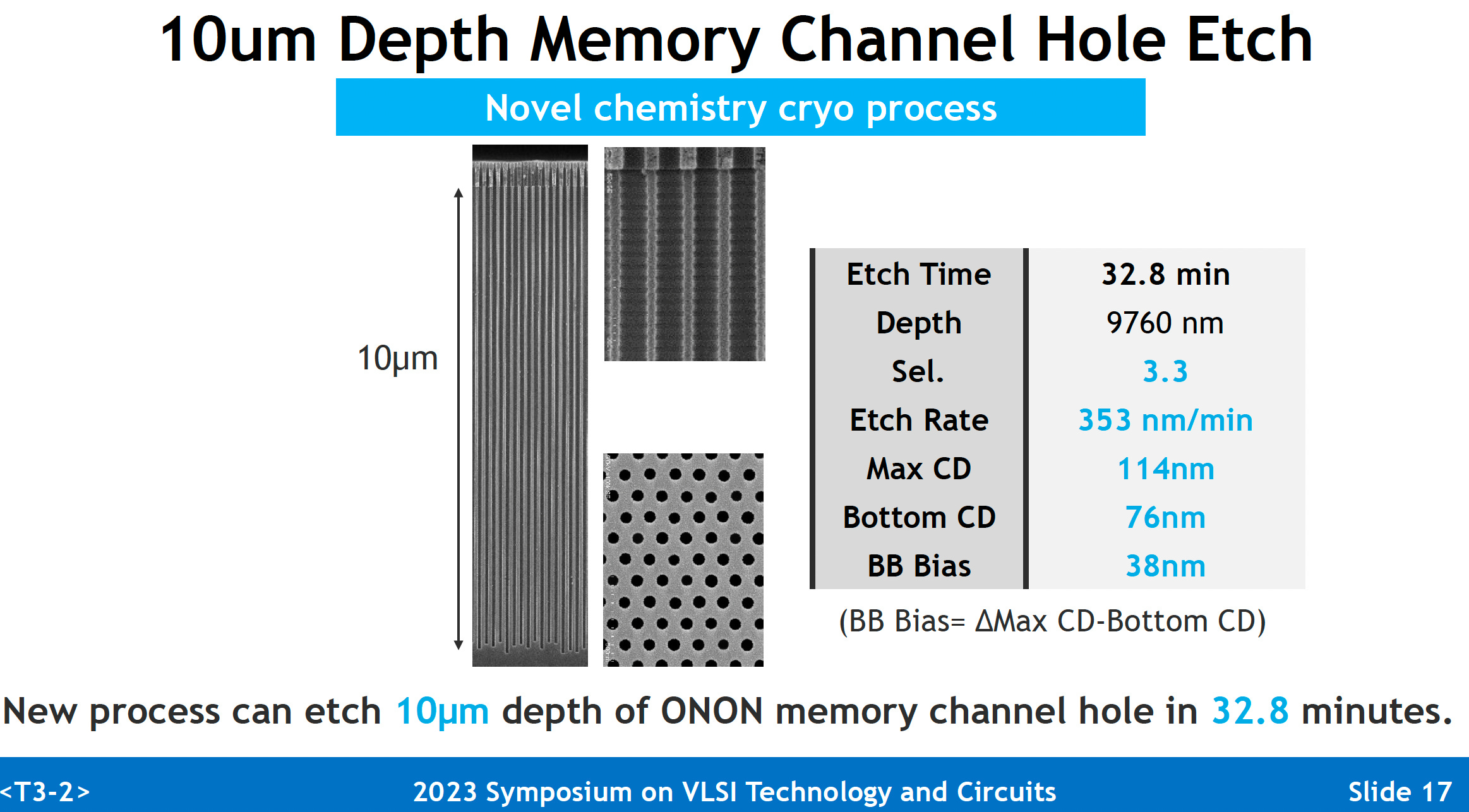
The current conventional method can etch to a 7-8 micron depth, taking about an hour to hit that depth. So Tokyo Electron’s process is faster and better than the previous solution. That’s a meaningful improvement in throughput.

This innovation is not lost on NAND companies. Kioxia and WD presented a 300-layer single-stack NAND technology, and most of the major customers will likely evaluate this in their technology roadmaps at some point. By moving to a single deeper single-stack NAND technology, memory companies can save more money on processes while still scaling to deeper memory. It’s going to be revolutionary for the NAND companies in terms of cost-downs in the future.
The summary is this: Tokyo Electron’s new cryogenic etch tool is 2x faster at etching a hole that is 25% longer than the previous process. It’s taken them some time to bring this product to market, but almost all NAND companies are likely in discussion with Tokyo Electron. This is going to shake the NAND industry structure.
For more thoughts on competitive share shifts and thoughts about companies, I have a brief competitive analysis behind the paywall.
