VLSI Japan: It’s Better on the Backside
Intel announces its PowerVia technology, and scaling the backside is the next big thing. This could be Intel's moment.
Hello from Kyoto! If there was a single big story from VLSI this year, it had to be Backside Power Delivery (BSPDN). VLSI is one of the premier conferences for semiconductor design and has been held since the 1980s. Today it’s one of the best places to present cutting-edge research in circuit technology. The key revolutionary announcement at VLSI this year was BSPDN. Let’s discuss.
Almost every session for BSPDN was considered the main track, and the BSPDN workshop, the main track, and almost all the attention of semiconductor professionals was focused on this big inflection. I wrote about BSPDN last year, and it’s one of my favorite things I’ve written, but I thought I would take another stab at explaining BSPDN from the ground up and then cumulate in the announcement of PowerVia.
What is BSPDN?
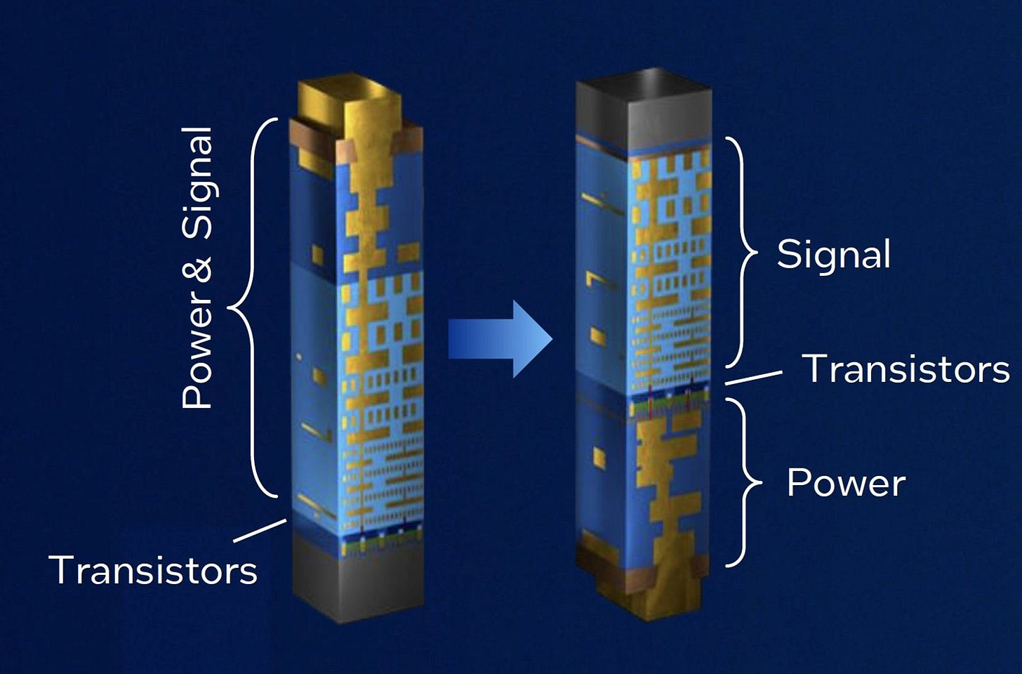
Backside Power delivery refers to splitting the signal and the power layers in a semiconductor chip. Let’s look at an image to help you understand what that exactly is and why that matters.
Note that this takes two wafers and is a process of fabricating the front side, flipping the chip over then bonding the wafer to another wafer with the power layers. This effectively creates a single device consisting of two parts “glued” together with hybrid bonding.
Chips up until this point were made with the bottom critical transistor layer first, and then successive layers of signal and power were built on top. The signal is the electrical signal that is wired to a transistor to tell the transistor layer what action or data to compute, and power is the source of current to power the transistors. Signal and power must be scaled to larger dimensions for better signal quality, power distribution, and thermal dissipation. But there’s been a problem on the power side called IR droop.
Defeating IR Droop - Why BSPDN Matters
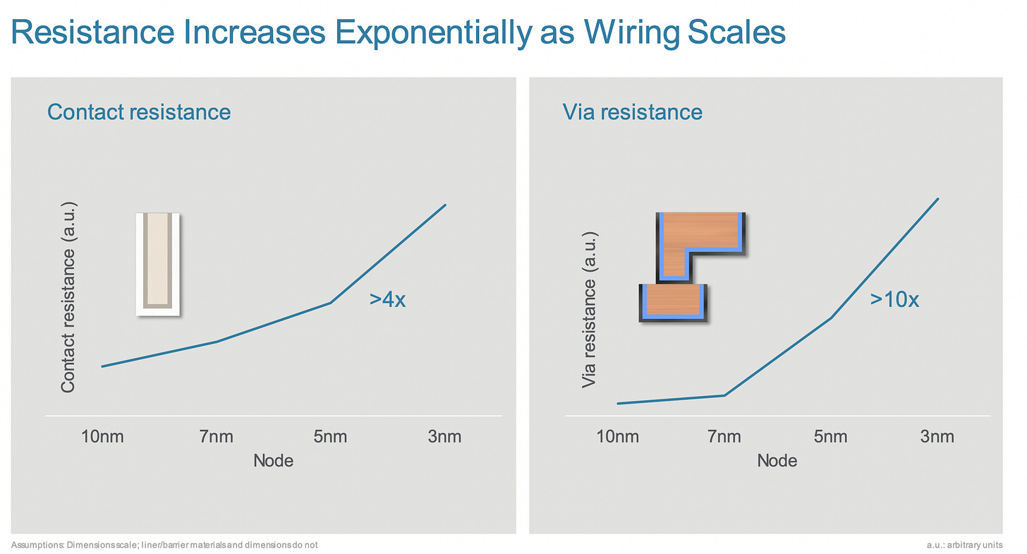
As energy flows through an electrical wire, resistance increases as the wire gets smaller and smaller. In the case of semiconductor design, recently, that resistance has gone parabolic and has hit a wall in 3 and 2-nanometer design. This is called IR droop.
This is where the IR droop problem has become a brick wall. The smaller features of 2 nanometers, in particular, made it so that the electricity could not reach the transistors to supply the transistors adequately. So the clever idea of BSPDN has now come to the forefront.
BSPDN is a solution to the IR droop problem and a novel semiconductor design. One speaker at VLSI called it the “dark side of the moon,” which refers to the backside of the wafer. The history of semiconductor manufacturing until now has been printing designs on just one side of the wafer. What if we could split the intricate wires and routing layers into power and signal and then put the power network on the backside? That’s the core of BSPDN.
This added cost and complexity wasn’t done willingly. IR droop forced the industry to decide, but now that this new technology is being adopted, companies are adapting it at different rates. Surprisingly, the company in the lead is Intel, and that timeline focus was the core of my recent piece about how I see Intel’s turnaround inflection point.
Intel is making bold bets and adopting PowerVia before TSMC. By doing it with RibbonFET (their adaption of GAA), Intel should be able to leapfrog TSMC’s process and get back in the lead. The stakes couldn’t be higher.
PowerVia is How Intel can beat TSMC.
Intel is making this bet completely alone. TSMC’s insertion of BSPDN will likely happen as late as 2026. Meanwhile, Intel is hoping to ship PowerVia next year. Intel is betting the farm on PowerVia, and as you can see below, if they ship PowerVia in 2024, it will be two years ahead of TSMC.
Intel is bold and pushing forward with BSPDN, and the leadership position couldn’t be a harder position to be in. They must create their own debug tools, optimize new EDA flows, and pursue the path alone. If they can execute, they will have a real competitive advantage. I want to talk about the technical benefits and challenges of PowerVia because it’s not trivial.
Technical Challenges and Benefits of PowerVia
PowerVia is a completely revolutionary technology. I think the best analogy for most of my readers is EUV. But not only is it a process change, it is also a huge design change. There’s a difference, but I will broadly use the EUV analogy for what will happen.
When TSMC adopted EUV into their process, they were the first to ramp up and had to do the hard process of learning the challenges of EUV. Particularly the EUV mask contamination and some of the resists were a whole new set of problems that were hard to solve. And when you’re first to start the path of a new process change, you have to figure out the entire process yourself. EUV insertion at Intel took years, with Intel 4 being the first node with EUV in 2023. Meanwhile, TSMC inserted EUV in 2016. It took Intel 6 years to get EUV in the process, and part of that difference is clearly because of the problems of scaling new technology in conjunction with a broken culture.
BSPDN will be a similar magnitude of process improvement. Intel will be inserting a more aggressive form of the technology than TSMC eventually will, but over two years in advance. This will not be quite the lead that EUV afforded TSMC, but this will be a meaningful gap between the processes. What’s more, unlike EUV, I think that there’s a chance that BSPDN has multiple opportunities for design advantages for years to come. BSPDN has completely opened up the wafer for more evolutionary design changes.
Technical Challenges
BSPDN will likely be a much simpler technology transition than Gate-All-Around (GAA) in terms of process. But because it’s new, there are some real challenges that I think are not trivial and will take some time to solve. A few big classes of problems are debugging, thermal, and design. These are non-trivial and are on top of the comparatively simple process problems.
Debugging and inspecting the problems for BSPDN is one of the most interesting problems. Intel called it a “Black Swan” event as many of the tools they had to debug had to be created from scratch. Intel notoriously spent less on process control, but this is an even harder class of problems. All the tools for debugging and EDA design tools are made for front-side design. Intel has to not only figure out how to yield the process but how to figure out how to scale the process.
To debug, Intel had to learn new techniques to deal with the thick metal layers in front of transistors and new models to account for the new design changes. The back side is a new design feature and the current architecture. EDA tools for the backside will likely be first standardized on Intel’s 18A process before anyone else, and while EDA vendors do try to make their tools standard across processes, Intel being first is important.
Thermal management is another huge challenge, and one of the most interesting aspects is that it seems like Intel has managed to scale PowerVia in line with Intel 4’s process for temperature rise. Temperature is one of the consistent worries about backside power, as the buried layers of transistors will be much harder to cool, and more layers create more problems.
This graph was surprising as they managed to show that temperature was in-line with a scaled Intel 4 (non-BSPDN) design. AMD’s engineers at VLSI immediately asked them how they could do this, but the answer, it seems, is proprietary. Intel has some secret sauce they are unwilling to divulge, and they will use these new advantages to be even more aggressive. If Intel can ship PowerVia and RibbonFet, they will be the undisputed leaders in the process. I want to focus on some interesting impacts from Intel aggressively pursuing BSPDN as they will have a competitive advantage in process and cost going forward. It’s worth discussing.
Competitive Advantages and Benefits
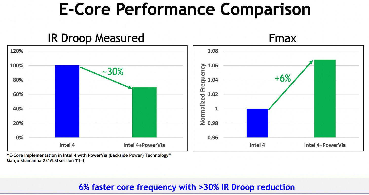
I allude to it above, but I think the early adoption of PowerVia has a two-fold effect. First is performance. I have been alluding to the performance benefits the entire time but have yet to quantify them. Let’s do that now. First, IR droop decreases 30%, while performance increases by 6% per core. This is important scaling performance with less energy, one of the most important bottlenecks in the semiconductor process.
I want also to mention that the 30% includes some off-the-shelf IR droop testing units, so they feel that they can comfortably get closer to the 40% that they modeled when they ramp the process.
BSPDN's primary goal is to increase power to the cells, which can improve many aspects of the performance. A good example of the improvements offered in signal length reduction. Lowering the signal's length leads to better routing, and we waste less energy giving instructions through circuits. By lowering the length of the signal, we improve energy efficiency. One of the problems of a deep and complex front-side signal network is porpoising, which is when the signal goes up and down the signal layers and creates needless complexity. BSPDN solves this.
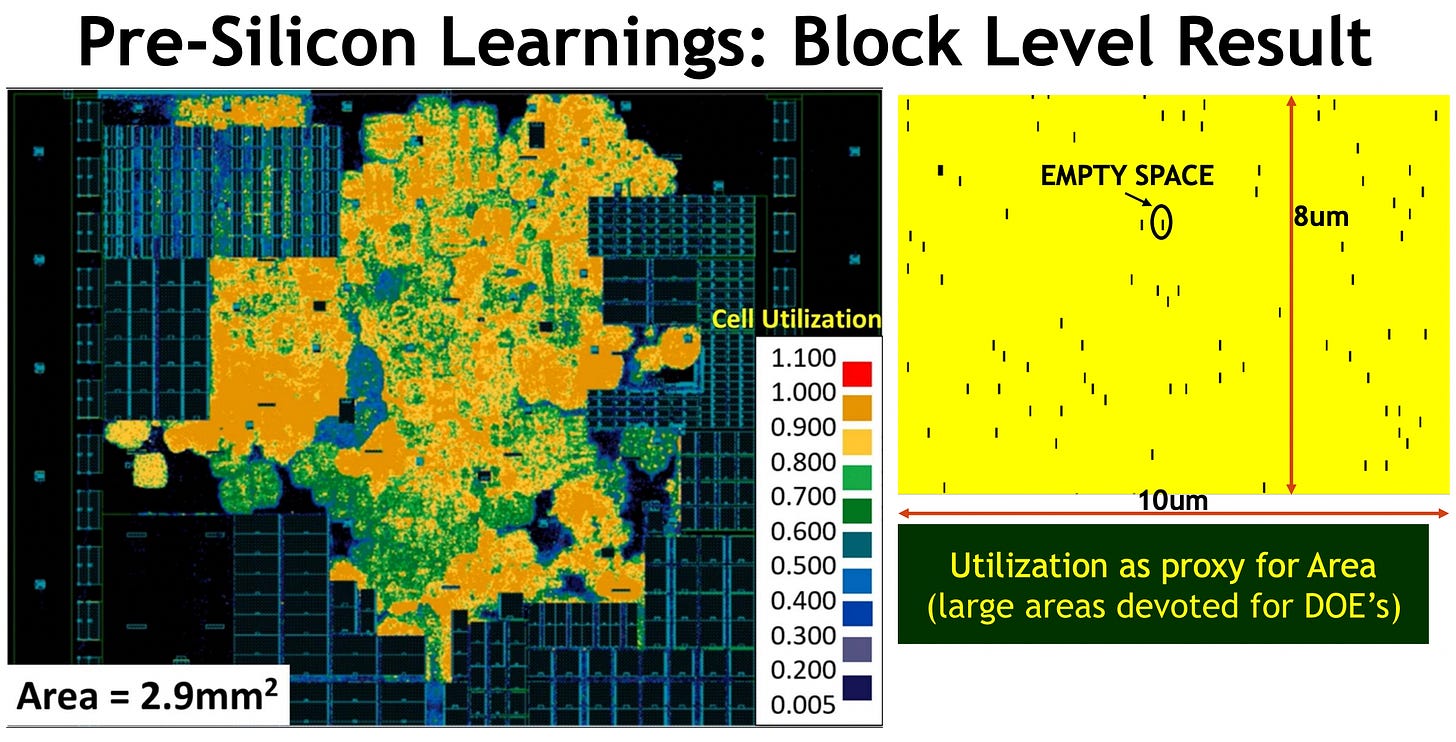
Another benefit is that the density of active transistors can scale much higher by having better power utilization. Cell utilization is much higher than Intel 4, which is driven by the power that can reach each cell, leading to better effective utilization of the transistors on the wafer.
Utilization of the transistors is coming when there is less utilization in the metal layers, meaning that the network itself is less loaded. That will be important for future functional backsides (I discuss that briefly). Think of it as this complex system is now running much more efficiently, as the network has much less traffic to do the same thing. That new freed-up space will be utilized for better performance.
Another aspect of BSPDN that is interesting is that there is a slight cell shrink. Cells are the standard unit of a transistor that is printed into the wafers, and if you look at the below data, PowerVia has less cell height, which means that there will be transistor “shrink” enabled by better design. Backside contact will take this to a whole new level.
The net effect is that PowerVia is an evolutionary technology, and Intel has put its entire effort into this product. They will perform better, which can be reinvested into the design process to lead to faster transistors. Between higher utilization, cell shrink, and relaxed metal pitches, there are so many ways to win with PowerVia. And Intel will have the most aggressive roadmap in this technology for years to come. If they can deliver high-volume manufacturing (HVM), they will take the clear leader in the process once again.
I also want to talk about the softer side of BSPDN because I think there is a subtle design advantage here. EDA tools will be optimized first around Intel’s process, which means that going to market likely will be faster for the complexity of circuit design at Intel than TSMC when it comes to BSPDN.
Moreover, they will also be pursuing Backside Contact (BSC) much sooner than their peers, which makes sense since they were first to BSPDN and PowerVia, while peers are focused on ramping Buried Power Rail (BPR). BSC, in particular, offers much better cell shrink advantages and alone could account for a cell shrink. I’m trying to say that being first to PowerVia means they will be first to BSC.
This looks like a sustainable lead to me in the process. TSMC, for example, will have a 2-3 year lag for BSPDN, and even then, they will be adopting a more conservative BPR approach than Intel. So in 2 years, they will still be “behind,” everything else equal. I want to highlight that this isn’t a flash in the pan, and TSMC cannot magically catch up to Intel from nowhere. PowerVia seems to be a very long time coming. Look at the defect density chart, it starts in 2021. Intel has been working on this process for three years.
There’s a lot of non-trivial design processes that will take time, and as they optimize better aspects of the EDA routing for Clock Tree Synthesis, more clocking on the backside, and eventually even a functional backside. Intel hopefully has time to figure out what to do with the new backside afforded to them, which can mean they have a sustainable process advantage.
Intel’s Potential Competitive Advantages
I want to now talk about how this translates to competitive advantages. The first I want to talk about is cost because it looks like this will cost a lot less than you’d expect. This flies in the face of what you’d think because the increased complexity is important coming in with fewer EUV layers.
By splitting the power to the backside, it looks like the metal layers underneath will be a much more relaxed pitch, meaning less EUV and lower cost. Intel says this saves them money, which is an amazing insight. They are going to be leading in technology with a cheaper process. That sounds like a competitive advantage for IFS if they can get customers to use their process more.
Another aspect is the process improvement because PowerVia will be a much better product. While we haven’t seen the performance of a ramped product, I would expect that PowerVia offers meaningful benefits over TSMC for lower-power products. That’s a big deal given the energy efficiency needs in an advancing world. That’s an advantage that Intel will have over TSMC for at least two years.
Another thing I want to talk about is the push to all-in PowerVia, which means the future is nearer for Intel because one of the most exciting roadmaps for BSPDN is the move to a functional backside. I want to talk about functional backsides and the future briefly.
The Future: Backside Clocks and Towards a Functional Backside
One of the more interesting comments about BSPDN is that the backside is overbuilt. This means there is more overhead for energy or electrical signals to move through the metal network connecting the power to the transistors on the backside of the chip.
This is like finding a “free” source of compute, and thinking about logically using this makes a lot of sense. The first thing that will likely happen is that the top-level clock of the Clock Tree Network will move to the backside, which frees up the signal side even more. This is a huge revolution in design and will make the complexity of the BSPDN schemes skyrocket, even as the simplicity of the design frees up space.
This is very good for EDA companies, as they will become even more important in this paradigm. There is a desire to push more function onto the backside over time, and this push for a symmetrical functioning wafer side will likely open the potential for design much further. One of the stated desires is to use BSPDN as a basis for 3D ICs, as there are new unused metal interconnects that can be stacked with HBM or other potential uses over time.
This is again another revolutionary step in potential design, and being the first to have BSPDN tinker with potential 3D IC designs is huge. This two-year period that Intel has BSPDN while TSMC does not could be a period where the lead lets Intel take the lead in future battlegrounds for semiconductor design, namely 3D ICs. BSPDN quite literally opens up the wafer for so much more potential, and being further down this path is Intel’s opportunity. What they choose to do with this lead could be revolutionary, but squandering it could be losing the future. Good luck with the execution Intel.
Last but not least, I want to put some thoughts about Intel and other stocks behind a paywall. There are some interesting read-throughs to semicap, EDA, and metrology.


