IEDM: DTCO & More than Moore
IEDM is showing how DTCO will overcome the end of Moore's Law.
Hello from San Francisco! It was a great week with all the papers at IEDM (International Electron Devices Meeting), so I thought I’d have some high-level takeaways of things I learned that I thought were interesting. First and foremost -almost nothing at IEDM has any impact in the next five years. A good rule of thumb is that when you see it at IEDM, you might see it in high-volume manufacturing in 10 years. But on the flip side the most consist investment advantage in this subsector is being ahead of the trends and inflections years before the market appreciates them. IEDM is the perfect forum for that.
IEDM at it’s core is about the future. Semiconductor scaling is a hard endeavor, and the complex decisions about the future of manufacturing, design, and semiconductors has to be debated years in advance. This is the forum for that debate.
Given that we have an investment time frame here at Fabricated Knowledge, I want to focus on a few things I found interesting that are huge inflections in a medium-term time period. Most of these have a public company that benefits.
The first big one and the one I want to spend the most time on is Backside power delivery networks. You're missing the point if you think EUV is the only game in town. The future is about Design Technology Co-optimization (DTCO), and Backside Power Deliever Networks (BSPDN) is a huge part of the roadmaps forward post-gate-all-around.
Backside Power Delivery Network: Scaling and More
A good place to start on what exactly Backside Power Delivery Networks (BSPDN) is is my post I wrote a few months ago about the bold bets Intel is making there.
The big takeaway is that BSPDN is clearly going to be inserted in the design processes, and there is a small roadmap of improvements afforded by BSPDN. But after that, BSPDN will change the design process to allow adding more features, like moving functions on to the backside of the chip. By splitting the signal and power layers, there’s a whole new set of ideas of how to design chips with the space afforded from the power layers. This is Design Technology Co-optimization (DTCO) and System Technology Co-optimization (STCO) at it’s best.
BSPDN looks like it has several years of obvious scaling potential, so it will be a huge part of the incremental semiconductor process from here until 2030. It will not only improve the energy delivered to the chip, but actually shrink the cell size. Think about it like a new way to organize the room, and now we can fit more in less even though its the same room filled with the same objects.
Next, the roadmap in the long term after we have fully achieved backside power contact networks means we could open up the wafer on the other side of the chip. If we are opening up the other side to be a functional signal layer, there’s a potential we can start adding backside devices to the chip! This blew my mind, and the options for stacking layer, memory, and other devices (like energy capacitors) is endless! This is huge!
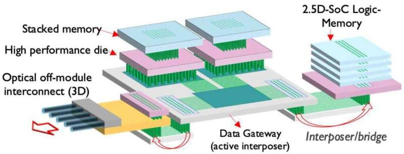
The first example given is by bringing metal capacitors on to the backside package itself, further extending advanced packaging. This time instead of 2.5D or interposers, the actual chip itself can extend to more devices because we will have a front and backside wafer, allowing more space to add functions.
And even more, we can start to add stacked memory directly into the silicon die because of the extra space and signaling room BSPDN affords. This is a very dense and interesting heterogeneous future offered only by BSPDN. It’s one level denser than hybrid bonding processes, as it’s actually built into the front end of the semiconductor process.
Eventually, BSPDN is going to complement the logic device roadmap, meaning that the density of gates will improve through the transition to nanosheet, then forksheet, and CFET, at the same time adding denser BSPDN insertions. The combined effect is a way to scale even amid the hard technical challenges that GAA and Forksheet offer. GAA will be a long node, with multiple generations akin to FinFET. BSPDN will make scaling with GAA more akin to traditional density scaling.
BSPDN in net is a trend that is as important as EUV scaling and will likely be one of the most powerful and incremental toolkits in scaling silicon in the future. Luckily the beginning of BSPDN is happening soon, and its eventual evolution is something to focus on. Applied, for example, think it’s meaningful for their metals deposition business. According to Gary Dickerson in their last earnings call:
Wiring is probably the #1 focus, and I don't know that everyone really understands how important that inflection is for our customers. That's an area where we have tremendous strength. We're enabling a 50% reduction in wiring resistance with integrated platforms that combine many technologies together.
This story is a big one. It’s as important as ALD and hybrid bonding and will be a huge new vector of improvement. It’s going to be incremental, so the more articulated vision will likely yield winners and losers for the future of WFE spending. Applied’s historical dominance in the metals deposition business has them well positioned for now, but other winners are likely to emerge.
Hybrid Bonding is the Near Term Process Inflection
Hybrid bonding must have been uttered in every other talk at IEDM. While some did still defend the viability of TCB in cost usage, hybrid bonding clearly is the advanced packaging process that the big 3 foundries will be pursuing. Both Intel and TSMC will be introducing hybrid bonding to their process, and TSMC said they are optimistic and not seeing any real problems with the process.
Tokyo Electron, in particular, had a great series of talks about hybrid bonding. Hybrid bonding, and even fusion bonding (SiO to SiO bonds), could be a huge driver forward for logic and memory scaling in the future. What’s interesting is that so far, the only hybrid bonding has been done primarily in CMOS image sensors, a wafer-to-wafer application while in the future, there are now die-to-wafer (D2W) and wafer-to-wafer (W2W) configurations.
Both methods have their benefits. D2W allows for complexity and heterogeneous options, like multiple smaller chiplets on a larger piece of logic. Wafer-to-wafer is simpler and more precise because of better overhead placement and scale, but so far die wafer seems to be the primary technology driving the SOIC (TSMC), Foveros Direct (Intel), and Samsung solutions.
The reality is it looks like both wafer-to-wafer and die-to-wafer will be used. It’s a big market, and its a clear that it’s going to be one of, if not the most important driver for heterogeneous logic density in the upcoming generations. It’s expected to be one of the fastest growing segments in WFE for the near term. Here’s a chart by Yole for example. W2W will be the bigger market, but D2W is growing off a much smaller base. There’s a chance these numbers end up quite conservative.

There are essentially two big “schools” of hybrid bonding. W2W which is mature and mostly done by the EV group and Tokyo Electron. Meanwhile the clear leader of D2W is Besi and Applied’s coupled tool. I have been bearish on BESI in recent notes, mostly focusing on the problems near term of packaging. Given I think that Q1 is actually the bottom for the semiconductor industry, it’s time to flip bullish. BESI still is one of the few companies where I think they could easily double their revenue in the next few years, and the multiple is not very demanding. I am very bullish.
For more on a very simplistic way to think about Hybrid Bonding at BESI, refer to this writeup. The math likely is conservative, and that much potential torque for a semicap company should be very bullish.
Both W2W and D2W will do well, but I think there’s no other pure play in this market. I wish EV Group was public. BESI is the best public option right now.
TSMC FinFlex 3nm Process and Hetegenous Process
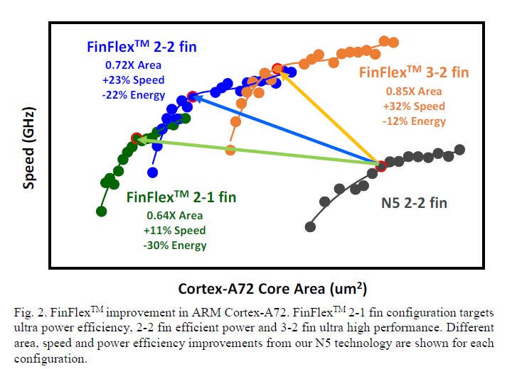
Last but not least was the release of the new 3nm process and the details about the products for the new FinFlex platform. It’s an interesting exercise in DTCO, because instead of just offering the single cell format layout, they are offering custom cell variants. A reminder for readers that cells are a unit of design of the gates of semiconductors at the smallest level of of a semiconductor.
What TSMC did that was so interesting is offering 3 different types of cell design types. The 2-1 Fin is only 11% faster but is 30% more energy efficient. While the 2-2 fin configuration is ~20% faster with 20% better energy performance, and the 3-2 fin is maxed out in performance at 30% better performance but only 10% energy improvements. Each of these custom types of fins offer specialized performance improvements, and that’s quite ingenious.
The different design types likely makes design more specialized, but by choosing the correct fin type for the correct application, customers can get better silicon for their needs! In addition I would guess this confers some kind of moat in terms of design types for TSMC. I don’t know if Intel or Samsung will offer the 2-1 and 3-2 fin types, it seems unlikely.
Another important consideration is that it seems likely the 3nm node is the last FinFET node at TSMC, and setting up different types of FinFET with better energy and performance types likely helps the longevity of this node. Pursuing smaller geometeries is hard, and more companies will fall to the wayside. 28nm was the last planar node and is effectively the golden node for price to performance for most trailing edge performance. 3nm will likely also be around for awhile, and having different “types” of 3nm will increase the longevity of this node. Unless you’re making super advanced logic, more applications will get caught up in the last great FinFET node; 3nm.
I wasn’t sure what to expect from the FinFlex announcement, but I thought this was massively clever and something that hadn’t happened before. We are really entering a new age of DTCO, and even concepts like standard cell sizes are being evaluated. Why not? Moore’s law is over, feature scaling is topping out, it’s time to get creative. And the FinFlex platform is a perfect example of that.
I hope you notice that all three trends I talked about are not about EUV scaling, but being more creative with the toolkit semiconductor engineers have to design chips. That’s the future, and it’s one that will be clever and much more varied than the undifferentiated planar scaling of Moore’s law.
That’s all for this week - sorry for the long delay. Sickness into a conference really delays your ability to write (or at least mine). I will have a piece about Marvell’s industry analyst day, an update of the China and segment comp sheet, as well as hopefully a dive into a company I find really interesting soon. I was lacking ideas for a second, and now I have too many!
If you found this useful - consider sharing and subscribing.


Will there be a follow up article on stuff that are not so imminent ?😀
So much nerdery! Thanks! 💚 🥃